Logo specs-groupDetail

ARPES

Angle-Resolved Photoelectron Spectroscopy detects valence band electrons emitted by irradiation of a sample with UV light due to the photoelectric effect. Highest resolution detection of the energy and angle distribution of the photoelectrons allows to determine the electronic structure of solids.

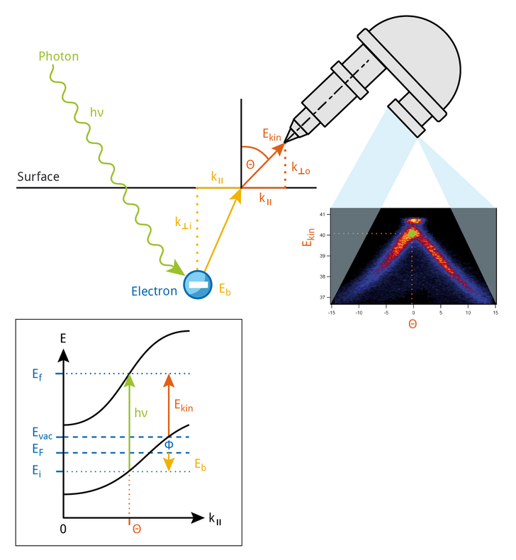
Photoelectron spectroscopy (PES) is one of the most powerful and most frequently used spectroscopic techniques in solid state physics, physical chemistry, and materials science. Using the photoelectric effect, PES provides a material-sensitive and non-destructive probe for modern scientists to examine the chemical composition (XPS or ESCA) and the electronic structure (UPS and ARPES) of materials. By illuminating a sample with light of a certain photon energy (hν), electrons are released from a solid using the photon energy to overcome their binding energy (Eb) and work function (Φ). The remaining energy provided by the photons is transformed into the kinetic energy (Ekin) of the photoelectrons. Such a transition can only occur from occupied electronic states of an energy Ei into unoccupied states of energy Ef because of the energy conservation rule.

Ekin=hv-Eb-∅

In the special case of UPS and ARPES, only electrons of the topmost electronic states, close to Fermi level, are in the focus of the analysis. Those electrons form the conduction band (valence bands and surface states) in the case of metals and semiconductors and are of special interest for modern materials science. Their wave vector (or momentum) k ( kx, ky, kz), and the energy has to be conserved during the photoemission process. This leads to different characteristic emission angles of the electron from the surface, depending on their momentum inside the material. As a result, it is possible to record the photoemission intensity (I) as a function of the kinetic energy (Ekin), providing the chemical/energy information, and the emission angle, providing the momentum (k) of the electrons.

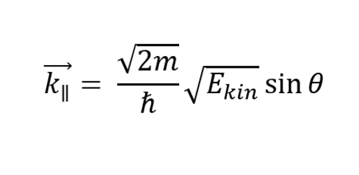
The surface breaks the geometry, not affecting the energy conservation rule, but affecting the momentum conservation such that the parallel wave component kӀӀ (meaning kx and ky) is conserved after crossing the surface whereas the component along the surface normal (k) is not conserved. The electrons can be analyzed in an electron analyzer with respect to their Ekin (or recalculated to Eb) and to Θ (or recalculated to the parallel wave vector component (kӀӀ). On this basis, a 2D distribution of the electrons for given Ekin and kӀӀ is measured, directly reflecting the electronic (or band) structure of the material.

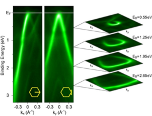
Modern analyzers and surface analysis systems offer the possibility to access a second emission angle by tilting the sample along the y-axis or by using an integrated mapping deflector inside the electron lens (for example the SPECS ASTRAIOS 190). By shifting the emission angle in the second dimension, it is possible to acquire a two dimensional band map in the dimensions kx and ky. The out-of-plane momentum kz, can be accessed by changing the photon energy of the excitation light source. 

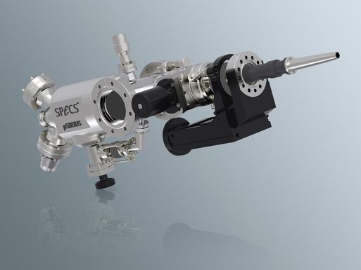
The ASTRAIOS 190 is a modern single deflector analyzer with a wide angle acceptance lens and a motorized entrance slit. It is designed to measure a large fraction of the angular (momentum) space by its large ±30° acceptance angle. Combined with the deflector technology, a large fraction of the band structure can be measured. Compared to older type analyzers, this is up to 4x more Information obtainable in one experiment. The deflector is based on a new approach using a single deflector approach enhancing the precision compared to existing dual deflector type analyzers. The motorized entrance slit mechanism supports fully remote operation of the analyzer and allows to separate the slit from the physical entrance of the hemisphere. In this way, best imaging quality can be combined with best eneryg resolution.  

Such experiments in laboratory environments require intense, small spot UV light sources of high stability for optimum performance. The intensity of the light source is the key point for fast and efficient measurements while small spot sizes ensure measurements with highest angle (or momentum) resolution. SPECS offers a series of UV sources fitted for various demands, starting from flexible and robust UV sources for economic application to highly sophisticated UV sources for different gases and photon energies with monochromators for highest performance and energy resolution.

In addition to the energy and the momentum, further dimensions can be taken into account for scientific analysis such as the spin of an electron or even the real space origin for small spot analysis (see momentum microscopy). Using a spin sensitive detection unit, it is possible to measure the intensity difference between the electrons of majority and minority spin (spin up and down) and calculate the so called asymmetry function. 

For the interested reader: It is good to know that in ARPES (and in photoemission in general) the collected electrons originate from an excited state. However, in most cases it is a good approximation to assume the final state is similar enough to the ground state to make conclusions about the electronic structure of a solid. 

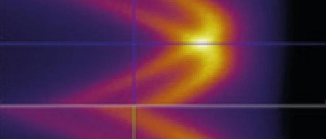
Demonstration of the ASTRAIOS 190 single spot shifting lens. On the example of Graphene/SiC, excited at He II (41.2 eV) photon energy with a monochromated small spot UV source, the effect of using the deflector is shown. 
RELATED PRODUCTS

56

APPLICATION NOTES

Overlayer Quantum Well States
Angle-resolved one-photon photoemission was used to investigate angular resolved photoemission from Ag overlayers on Cu(111).
download PDF
Resolving Power of the PHOIBOS Energy Analyzer Series
The line width of Xe and other rare gas levels using the SPECS gas cell UGC 10 and the SPECS UV-light source UVS 10/35 has been measured. The special geometry of the cell includes space charge compensation electrodes to demonstrate the ultimate energy resolution of the PHOIBOS analyzers.
download PDF
Ultimate energy resolution of the PHOIBOS Energy Analyzer series
We have measured the line width of the Xe 5p3/2gas line using the SPECS gas cell UGC 10 and the SPECS UV-light source UVS 300. The special geometry of the cell includes space charge compensation electrodes to demonstrate the ultimate energy resolution of the PHOIBOS analyzers together with the 2D-CCD Imaging Detector.
download PDF
PHOIBOS 150 2D-CCD Wide Angle Mode in 2PPE
These notes describe the application of the angular resolving wide angle lens mode (WAM) in two-photon-photoemission spectroscopy (2PPE).
download PDF
Ultimate Energy Resolution of the PHOIBOS 100 CCD
We have measured the line width of the Xe 5p3/2gas line using the SPECS gas cell UGC 10 and the SPECS UV-light source UVS 300. The special geometry of the cell includes space charge compensation electrodes to demonstrate the ultimate energy resolution of the PHOIBOS 100 analyzer together with the 2D-CCD Imaging Detector.
download PDF
Spin-resolved photoelectron spectroscopy
Spin-resolved photoelectron spectroscopy experiments were performed in an experimental station consisting of an analysis and apreparation chamber. The preparation chamber is used for substrate cleaning, as well as for the preparation and magnetization of ferromagnetic thin films.
download PDF
Photoelectron spectroscopy with UVLS and TMM 304
Angle-integrated and angle-resolved photoelectron spectroscopy measurements were performed using the SPECS UVLS ultraviolet-light source in combination with the toroidal-mirror monochromator SPECS TMM304, which was equipped with two cassettes of optical elements in order utilize the HeI and XeI emission lines with photon energies of hν=21.22eV and hν=8.437eV,respectively.
download PDF
Small Spot UV Source
High resolution photoemission measurements demand not only a highest performance electron spectrometer, but also a UV source with high flux density and small spot size, especially for angular resolved studies. SPECS has developed a focused UV source on the basis of the proven technology of the UVS 300 source. Using a special capillary, this source can be focused down to a theoretical spot size of 500 micrometers.
download PDF
Cross Section through the Brillouin Zone of Pb 2D Quantum Well State Bands
Examining unexpected properties of Pb, a free electron metal
download PDF
High Angular Resolution Data from the Band Structure of Thin Layers of Indium on Si(111)
The band structure of thin layers of indium on Si(111) was measured with ARPES. Due to electron confinement in the direction perpendicular to the surface, quantum well states (QWS) are formed. The experiments were performed at the BESSY II 10 m NIM beamline at the U125/2 undulator, which has an energy resolution of less than 1 meV, and a small spot size.
download PDF
Band Structure of Crystalline Graphite Layers on SiC (0001)
The band structure of crystalline graphite layers on the (0001) surface of SiC was measured by high-resolution angle-resolved photoelectron spectroscopy. The experiments were performed using a SPECS UV source 10-35, which has an energy resolution of about 2 meV and a spot size of about 0.6 mm in diameter. The photon energy for all measurements were 40.81 eV (He II).
download PDF
Fermi-edge of a single crystal TiTe2 sample at low temperature
The Fermi-edge of a single crystal TiTe2sample was measured at low temperature. The diode closest to the sample read 12 K. A sample temperature of 17 K was estimated. The data was taken with a PHOIBOS 150 CCD analyzer at 3 eV pass energy and with 0.2 mm slit width.
download PDF
Measurements of the Surface State of Au (111)
The band structure of the (111) surface of Au was measured by high-resolution angle-resolved photoelectron spectroscopy. The experiments were performed using a SPECS UV 10/35 source, which has an energy resolution of about 2 meV and a spot size of about 1.5 mm diameter. The photon energy for all measurements was 21.23 eV (He I).
download PDF
Measurements of the Surface State of Cu (111)
The band structure of the (111) surface of Cu was measured by high-resolution angle-resolved photoelectron spectroscopy. The experiments were performed using a VG UV source, which has an energy resolution of about 2 meV and a spot size of about 1.5 mm diameter. The photon energy for all measurements was 21.23 eV (He I).
download PDF
Quantum Size Effects in uncoupled Al layers on graphitized SiC
track Quantum well states, measure 2D band structure, parallel component of wave vector, 2D spectrometer use
download PDF
Two-Photon-Photoemission
This Note shows the one- and two-photon photoemission signal of the Cu(111) surface state at 300 K for the different angular resolved lens modes of the PHOIBOS analyzer at different pass energies Ep. The surface has been analyzed using a PHOIBOS 150 analyzer with the 2D CCD Detector.
download PDF
Close
Your web browser is deprecated
This could effect the presentation and some functions of our website.