Measurements on quantum dot devices with Nanonis Tramea
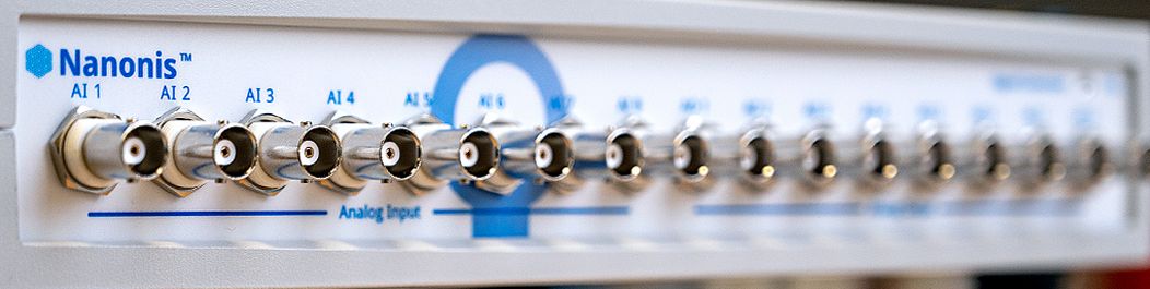
Nanonis Tramea is a fully integrated, high-performance, software-based quantum transport measurement system.
Quantum scientists at IMRE Singapore who engineer and investigate next generation materials and devices for use in quantum information processing applications recently published a paper in Advanced Materials. They report on a combined experimental and theoretical approach for the investigation of the nature of low temperature carrier transport in CVD-grown 2D WS2 devices with ALD-grown high-k HfO2 dielectrics. The studies were published in Advanced Materials.
Measurements on the quantum dot devices were performed with a Nanonis Tramea quantum transport measurement system in a Bluefors LD dilution refrigerator at a base temperature of <20 mK. Nanonis Tramea is a fully integrated, high-performance, software-based quantum transport measurement system.
Their study is the first demonstration of electrostatic gate defined quantum confinement of carriers in devices made on wafer scalable CVD materials and CMOS compatible dielectric processing and an important step towards practical applications. It also demonstrates the benefits of Nanonis Tramea, including high signal quality, high measurement speed and ease of use for characterizing multiple-gate nanodevices. In this case, such nanodevices can be used as key building blocks for unique spin–valley hybrid TMDC based qubits that could offer long coherence lifetimes and fast operation speeds in a planar architecture.
-------------
Researchers investigated influence of atomic layer deposition of HfO2 dielectric on different scattering mechanisms and carrier mobilities by performing temperature dependent transport measurements on the same set of single and bilayered CVD WS2 transistors before and after HfO2 deposition. Such measurements were possible thanks to the robustness of their devices against thermal cycling allowing scientists to clearly isolate the influence of dielectric deposition on low-temperature carrier transport. They have shown that low-temperature transport is not impurity limited as commonly thought, but rather due to another significant but often overlooked factor which is interface roughness.
Common metal–oxide–semiconductor field-effect transistors (MOSFETs) traditionally based on silicon as a channel material and silicon oxide as dielectrics are already at the limits when it comes to the scaling in size and complexity and new materials will be needed in the future for building more powerful electronics for quantum information processing. Recent studies have shown that 2D semiconductors such like transition metal dichalcogenides (TMDCs) are promising candidates for channel materials due to their novel properties being tunable layer-dependent direct bandgaps, strong photoluminescence, large spin–orbit coupling, and unique spin–valley coupling. Current state of the art MOSFETs manufactured by Intel contain high-k HfO2 gate dielectric for increasing gate capacitance with low leakage currents. The realization of functional and useful 2D TMDC nanoelectronics ultimately relies on overcoming challenges in material growth and device engineering, including dielectric integration. The presented study is providing key insights for improvement of 2D TMDC devices for useful applications.