Logo specs-groupDetail

SPM, STM, AFM

Scanning Probe Microscopy (SPM) is a group of methods, like Scanning Tunneling Microscopy (STM) and Atomic Force Microscopy (AFM), that uses a probe to sense a probe-to-surface atom interaction. By two-dimensional scanning of the probe on the surface, a high resolution microscopic image is produced.

Scanning Probe Microscopy (SPM), especially Scanning Tunneling Microscopy (STM) and non-contact Atomic Force Microscopy (ncAFM) in Ultra High Vacuum (UHV) or in defined atmospheres like Near Ambient Pressure (NAP) enable high resolution imaging and spectroscopy with atomic resolution. Stability is in state-of-the-art SPMs, like the Aarhus series, no issue. Results are reliably obtained on a daily base. Modern dynamic sensors, like the Kolibri-Sensor, even provide the possibility to measure STM, giving the access to the electronic information, and ncAFM, with access to mechanical information, at the same time. Combining this with the spectroscopic information single atom identification is possible. The Aarhus is also available in a NAP-version allowing studies of surface reactions at atomic level at the pressures between UHV and 100 mbar.

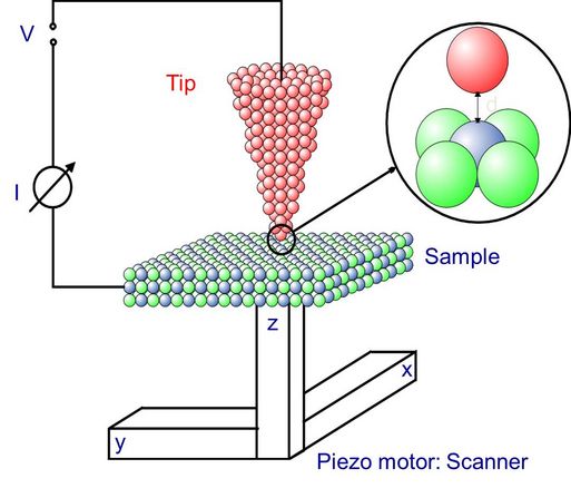
graphic illustrating the tunneling effect

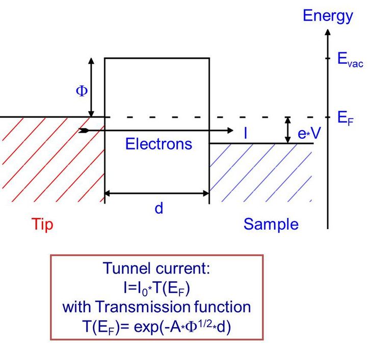
Scanning tunneling microscopy (STM) allows to map conductive surfaces on the nanometer scale by the use of the quantum mechanical tunneling effect. Hereby a sharp metallic tip (STM tip) is scanned across the surface at a distance of typically some tenth of a Nanometer. A bias voltage is applied to the junction in order to generate a tunneling current, which is used as feedback parameter and kept constant. As a result, the tip motion delineates along the scan direction a height profile proportional to the local density of states (LDOS) of the surface. When scanning line by line, a full 3D map of the surface can be reconstructed, even with atomic resolution. Due to the potential of this research technique, the Nobel Prize in physics was awarded to Gerd Binning and Heinrich Rohrer in 1986 for their development of the first STM together with Ernst Ruska. By means of STM, the surface's topography can be investigated, delivering information about its geometrical crystal structure, orientation of adsorbates and growth effects in real space. Thus it provides an intuitive insight into adsorbate-surface interactions, interface effects and, in general physics of surfaces with atomic-scale resolution. For moving the tip towards the sample and moving it along the scan area of interest two different approaches are implemented - both on basis of piezo motion. The coarse motor accomplishes the rough approach of the tip towards the surface, while the scan piezo is responsible  for the scanning motion. After transfering the sample object of examination into the sample stage, the tip is approached towards the sample´s surface until they are in tunneling range. During this process, the challenge is to perform the approach motion of several milimeters fast enough and still stop this course motion with such an accuracy that the surface is not distupted by the STM tip. The metallic tip is driven with sub-atomic precision over the sample with the assistence of piezo elements. The standard scan piezo design consists of a scan tube with its outer electrode segmented in four sections. That allows lateral motion in +/- X and +/-Y directions by means of voltage pulses applied to the outer electrodes and high precision vertical motion in +/-z with voltage applied to the inner electrode. Special care has to be taken to the stability of the instrument. When probing samples with sub-nanometer resolution the disturbace by outer impacts (i.e. vibrations or even acoustical noises) must not disturb the tip sample distance nor the sensitive electronic measures. Consequently, the stiffness of the equipment and ist vibration insulation are key characteristics of a SPM. In the case of the Aarhus SPM Series, vibration isolation measures are already implemented into the STM head, such that external vibration damping systems are generally not required to perform high quality STM or SPM measurements. The tunneling current, detected by a current pre-amplifier has an intensity in the order of nano-ampere. Thus it is very sensitive to noise disturbances and all signal cables must be shielded.

The feedback loop can be implemented by soft- or hardware. Usually it consists of a PI-controller (P: proportional term, I: integral term or time constant) where the set value is a given tunneling current (nA) and the control value is the Z-voltage. With the PI-Parameters the sensitivity of the controller can be tuned and adjusted to the acquiring speed for a topographic image. The Z-voltage is a measure of the sample' height at the position of the tip. This position can be recorded while scanning the tip over the surface pixel by pixel - line by line. The system's specific calibration defines the conversion of the relative piezo voltages to X,Y,Z coordinates in nm scale. Plotting the Z coordinate for each pair of X-,Y, coordinate in wrong-color representation visualizes the surface's topography. Under very stable conditions (no piezo drift/creep), and usually on very small scan areas, the above mentioned feedback loop can be switched off. In this mode, known as constant height measurement, the current signal can be mapped directly as a function of the X and Y coordinates.

The local density of states (LDOS) of the sample surface and adsorbates can be probed by STM spectroscopy with sub-molecular resolution. There are several spectroscopic techniques depending on how the three available signals, i.e., tunneling current (I), tip-surface bias voltage (V), and the tip-surface distance (z) are recorded. The most common spectroscopy technique to map the local density of states (LDOS) fixes z, and records I while ramping V through the occupied (sample at negative voltage) and the unoccupied (sample at positive voltage) states of the sample. The derivative of the current signal (dI/dV) can be obtained by modulation lock-in techniques and provides the LDOS. When recording the STS signal simultaneously to the normal topography the contribution of the LDOS to the conductance at a given voltage can be visualized in color representation displaying the bidimensional local distribution of occupied/unoccupied states at a given voltage (energy). The combination of STM and STS is realized by recording a STS I-V spectrum in each pixel of a constant height STM image. As a result a three dimensional data set is obtained, where individual layers represent topographic images at given occupational states.

With modern dynamic sensors, like the KolibriSensor, static and dynamic STM is possible, while at the same time the ncAFM signal can be recorded in parallel by the frequency shift in the vicinity of the sample surface being a measure for the force on the tip.

RELATED PRODUCTS

58

APPLICATION NOTES

High-Resolution Imaging and Spectroscopy of Water on NaCl(001) Surface
The interaction of water with the surfaces of solid ma-terials is ubiquitous. Many remarkable physical and chemical properties of water/solid interfaces are gov-erned by H-bonding interaction between water mole-cules. As a result, the atomic-scale description of H-bonding structure and dynamics is one of the most important fundamental issues in water science. Ideally, attacking this problem requires the ability to access the internal degrees of freedom of water molecules, which remains a great challenge due to the light mass and small size of hydrogen.
download PDF
Controlling QPlus small Amplitudes with Nanonis Setup
A growing number of users are opting for a modified setup of their STM combining a standard instrument with a QPlus Sensor to do non-contact AFM. QPlus sensors can be easily integrated with the existing STM head since they are based on oscillations of quartz tuning forks. The detection of such oscillations is done electrically and no additional laser system is required. When combined with low temperature this technique leads to a large spectrum of applications.
download PDF
Exploring Nanoelectromechanic of Ferroelectrics: PFM with Dual-OC4
Piezoresponse Force Microscopy (PFM) is now the primary technique for imaging, spectroscopy, and domain patterning in ferroelectric materials. Piezoresponse (PR) studies of ferroelectric materials has started in the beginning of 90s [1], and today undergo exponential growth due to rapidly emerging applications of ferroelectric and multiferroic materials for nonvolatile memories and data storage [2, 3]. These applications have stimulated extensive efforts toward understanding the mechanisms for polarization reversal in ferroelectrics on the nanometer scale.
download PDF
Non-Contact Atomic Resolution in Liquid Using Nanonis OC4
AFM imaging in liquid is often challenging due to poor quality factor of the cantilever and high environmental noise. With these challenges in mind, we constructed a beam-deflection AFM designed for imaging in various environments [1, 2]. Since we wanted to operate our AFM in frequency modulation mode, we combined the Nanonis OC4 (used as a PLL) together with the Asylum MFP3D controller and were able to obtain true atomic-resolution in liquid (right image).
download PDF
Automated Switching Between Non-Contact and Contact Modes of AFM
The study of plasticity by means of atomic force microscopy (AFM) is a fascinating experiment, as it is possible to observe the nucleation of single dislocations directly in the indentation force curve and image the resulting deformed surface structure with high resolution.
download PDF
OC4-Station and VEECO EnviroScope - Advanced Vacuum Measurements
Veeco EnviroScope combines a hermetically sealed sample chamber with scanning microscopy. Due to the relative high Q factor of the cantilevers in vacuum this instrument can be operated with an external PLL for advanced combined measurements, i.e. nc-AFM, MFM, EFM…
download PDF
Single Pass Kelvin Probe Measurement Technique in Air with Dual-OC4
The Kelvin probe technique is increasingly gaining importance in AFM measurements since it gives access not only to the topography but also to chemical information of the tip and sample. It is an extremely sensitive analytical method to detect changes in contact potential difference between different materials or chemical elements on the surface.
download PDF
Compensating for CPD in NC-AFM: AM-KPFM in UHV using Dual-OC4
Single pass Kelvin probe imaging (KPFM) gives information on the electronic structure of materials by measuring contact potential difference (CPD) while simultaneously acquiring topography. Under vacuum condition the Q factor is higher than in air, leading to higher resolution for both Kelvin and topography images.
download PDF
Far-Field Fibered Interference Scanning Optical Microscopy (iSOM) - Imaging Living Cells
In the field of biology, the scanning techniques in air or liquid environments are nowadays intensively used. AFM, STM, SNOM are relatively fast imaging methods allowing sub-µ resolution, in contrast with conventional optics allowing for fast and noncontact imaging, but suffering from lack of resolution according to Rayleigh criterion.
download PDF
Modulation of Contact Resonances: Use of PLL in Contact Mode AFM
Friction force microscopy (FFM) is a useful technique capable of characterizing material mechanical properties, such as elastic module, adhesion, and friction down to atomic scale. When combining static lateral force measurements with dynamic measurements of contact resonance frequencies the sensitivity is improved, i.e. subsurface defects are easier to detect than in conventional quasi static FFM.
download PDF
Friction Force Microscopy
Friction force microscopy (FFM) is a powerful tool which allows us to study the origin of friction in single asperity contacts. The observation of atomic stick-slip and its variation with load, during the sliding of tip against another solid surface provides detailed information about the dissipation mechanisms. Statistical averaging of repeated measurements with good control over experimental parameters is of crucial importance for reliable FFM measurements.
download PDF
Feenstra Type of Spectroscopy: Making use of the Programming Interface
Spectroscopic measurements in STM are an important tool for the investigation of the electronic states at surfaces. When combined with the variable tip-sample separation technique this type of spectroscopy leads to high dynamic range, 5 to 6 orders of magnitude, in the measured current and conductance even on the semiconductor surfaces with low surface state density.
download PDF
Improved Atomic Scale Contrast via Bimodal DFM: Dual OC4
Frequency-modulation atomic force microscopy (FM-AFM) is an efficient and already widely spread technique to obtain atomically resolved images of insulating or metallic surfaces. Typically, FM-AFM is based on scanning a sharp tip of a macroscopic cantilever over the surface, where the tip-surface distance is usually controlled by the frequency shit (f1) of the first normal resonant mode (f1) of the cantilever. The atomic-scale contrast arises from short range forces; e.g. covalent or ionic bonds, thus the detection sensitivity of the FM-AFMcan be improved by using small tip oscillation amplitudes comparable to the decay length of the short-range forces, ~ 0.1 nm. A lot of efforts are put in this direction in the FM-AFMfield, mainly based on the excitation of a tuning fork sensor or higher flexural modes of cantilevers characterized by largerstiffness.
download PDF
Atom Tracking used for Reproducible Force Spectroscopy
Force spectroscopy in dynamic force microscopy at room temperature is a challenging feat due to the unavoidable thermal drift. Especially in three dimensional force spectroscopy, even a tiny drift of around 10 pm over the measurement will result in a crucial error.
download PDF
Automated Amplitude Calibration in non-contract AFM Mode
Calibration procedures are always very important for correct quantitative measurements in SPM. In the absence of an interferometer, acquiring an accurate calibration using nc-AFM is complicated. The routine also has to be repeated multiple times for an accurate determination of the amplitude calibration factor which requires a non-negligible amount of time.
download PDF
Mapping the Orbital Structure of Impurity Bound States in a Superconductor
Superconductivity is a low-temperature phenomenon caused by the pairing of electrons via interactions me-diated by the environment. A signature of supercon-ductivity is that no single electron can be injected at low energies because the only possible states are the ones corresponding to pairs of electrons. Hence, an absolute gap in the density of states (DOS) is a finger-print of conventional superconductors. In s-wave su-perconductors such as lead the paired electrons (i.e. the Cooper pairs) have opposite spin. An external magnetic field forces the electron spins to align, there-by breaking the pairing and destroying superconductivity.
download PDF
Drift-Corrected 3D Dynamic Force Spectroscopy at Room Temperature
The ability to collect 3D dynamic force spectroscopy (DFS) data opens the door to valuable and more complete information of the interaction forces at the atomic scale. True site-specific atomic scale interaction forces and potential energies were accessible before mainly at low temperatures due to the absence of instrumentation-induced artifacts.
download PDF
Realization of a Tunable Artificial Atom at a Supercritically Charged Vacancy in Graphene
This is the first observation ever of a stable and tuneable charged vacancy in graphene and could allow researchers to fabricate artificial atom arrays for performing the electronic equivalent of optical operations.
download PDF
Supramolecular Rotary Device
For years a lot of efforts have been put on designing organic molecules whose properties can be exploited for building up artifi cial molecular devices. Together with our partners from the University of Basel and the ETH Zurich we created a specially functionalized molecule that on a Cu(111) surface does not only form a nanoporous network, but also have the right size to be nested on top of the pores.
download PDF
Trapped 2D free e- Gas of Cu(111) withinRegular Array of QDs: STS study
Two dimensional quantum confinements at surfaces have always been a challenge for the scientists, mainly because of the difficulties to produce regular nanopatterns that can trap electronic states. One possibility of analyzing such structures is Scanning tunneling Microscopy (STM) and Spectroscopy (STS) at low temperature.
download PDF
Femtogram Resolution for In-Situ Monitoring of FIB and E-Beam Induced Milling
The optimization of focused ion and electron beam induced processes for the reliable fabrication of micro- and nanodevices has been of increasing importance. For this a further understanding of the basic physics underlying the process is necessary. In-situ process monitoring is an efficient way to move forward in this field.
download PDF
Piezoelectric Quartz Tuning Forks for Scanning Probe Microscopy
In this paper the application of piezoelectric quartz tuning forks in dynamic force microscopy is described. For the introduction we give a historical overview and a comparison with traditional cantilevers. In the second section the theories for tuning forks as oscillators for the dynamic force detection are introduced and in the third section the experimental implementation is described.
download PDF
Spin Valves Investigated with BEMM - a Case for Nanonis`s Programming Interface
Recently a big effort has been put into the investigation of so-called spin valves, devices promising important advances in magnetic sensors, e.g. for hard disk read heads. Ballistic Electron Magnetic Microscopy (BEMM) is one method for investigating these devices. Electrons are injected through the tip of a Scanning Tunneling Microscope into a magnetic layer of a sample. The ballistic flow of electrons through the sample is studied at different magnetic fields while the tip-sample separation is controlled with the regular tunneling current.
download PDF
Optimizing PLL Feedback Parameters: Nanonis perfectPLL
Setting up a phase-locked loop (PLL) for use in non-contact applications is difficult. Four free feedback parameters for amplitude and phase control and two additional free parameters for the z-feedback leave a lot of room for incorrect settings and unwanted tip-crashes. Therefore we wanted to find a simple and reliable way to set up our PLL.
download PDF
Ultra-Low Current STM at 100fA
Scanning at ever lower currents is an ongoing effort in the STM community. In a test run at the University of Lille, the Nanonis control system was put to test with an Omicron-1 STM to measure atomic resolution images on a Si-111 sample.
download PDF
22-bit on all Ouput Channels: Nanonis hrDAC
In digital SPM control system the resolution of the digital-analog converters has always been a limiting factor, both in achieving atomic resolution and in spectroscopy applications. The newly developed hrDAC™ not only overcomes these limitations, but compared to the usual offset/gain approach, also has a series of other advantages.
download PDF
Integrating External Equipment - User Chanenels in the Nanonis SPM controller
We use the Nanonis SPM Control System and Oscillation Controller to operate our tuning fork-based JEOL microscope. The z-feedback runs on the frequency shift of the tuning fork. To make local capacitance measurements we attached a separately contacted metal tip to one prong of the tuning fork. In our effort to map local charge defects in Hf-based high-k gate films we had to integrate the signals from two ex-ternal lock-in detectors with the data acquisition of the control system.
download PDF
Doing Electrochemistry with an SPM tip: EC-SPM
Electrochemical SPM (EC-SPM) in liquid electrolytes provides an addi-tional level of experimental control for in-situ studies of surfaces and redox active adsorbates. Independent control of the tip and surface electrode potentials enables atomic resolution imaging and spectros-copy of electrochemical surface processes. This method allows for real-time analysis of electrochemical processes occurring at the electrolyte-surface interface as compared to ex-situ methods and has proven to be an invaluable experimental tool in the fields of electrochemistry and surface science.
download PDF
Single-Scan Kelvin Probe Technique in Air with Dual Oscillation Controller
In atomic force microscopy electrostatic forces are usually not discriminated against van-der-Waals forces. Attractive electrostatic forces cause the distance controller to retract the tip from the surface, resulting in erroneous height information in the topography image. Together with Nanonis we developed a novel solution to this longstanding problem.
download PDF
Atom Manipulation with Nanonis SPM Controller
Atom manipulation often attracts the interest of researchers, not only for observing artificial patterns on the surface, but also since it allows preparing ideal “samples” on surfaces, designed for a specific measurement. At the same time, however, it often requires a complete custom made scanning probe controller. Although the first systematic atom manipulation was demonstrated in 1990s, it is still challenging for mostresearchers. This application notes shows how the fully-digital Nanonis SPM controller with its LabVIEW Programming Interface can significantly reduce the technical challenges and simplify the manipulation process.
download PDF
Needle Sensor Operation in non-contact AFM Mode
Needle sensors are becoming increasingly popular to measure the tunneling current while not depending on the current for the distance feedback. A resonance frequency of 1 MHz insures a fast response of the sensor while interacting with the surface, but it requires a highly accurate Phase Locked Loop (PLL) to perform non-contact AFM measurements, especially with low frequency shift set points.
download PDF
SPM 150 Aarhus with KolibriSensor
On-the-Fly Switching Between STM and AFM - Topography Feedback
download PDF
SPM 150 Aarhus with KolibriSensor
Atomic resolution NC-AFM imaging with subangstrom oscillation amplitudes at room temperature
download PDF
SPM 150 Aarhus with KolibriSensor
Acquisition of atomic site specific force spectroscopy and two-dimensional force maps F(x,z) on KBr(001) and Au(111) at room temperature
download PDF
SPM 150 Aarhus with KolibriSensor
Atomic resolution NC-AFM on KBr(001)
download PDF
SPM 150 Aarhus with KolibriSensor
Atomic Resolution NC-AFM on Si(111)-(7x7)
download PDF
SPM 150 Aarhus with KolibriSensor
Atomic resolution NC-AFM imaging on Au(111) at room temperature
download PDF
STM 150 Aarhus "everyday" results
The STM 150 Aarhus is an outstandingly stable and time saving instrument for surface analysis. Even in noisy environments it shows ulitimate stability. The data shown in this application note are routine results as part of the standard specification procedure for all STM 150 Aarhus systems leaving SPECS.
download PDF
STM 150 Aarhus - High Stability Temperature Control
SPECS has developed a temperature design for the original STM 150 Aarhus system. Excellent performance in terms of mechanical stability and thermal control could be demonstrated for LN2 temperatures and temperatures exceeding 1000 °C.
download PDF
Close
Your web browser is deprecated
This could effect the presentation and some functions of our website.