Transport Measurements
Transport and nanoscale related phenomena triggered huge interest in scientific community after discovering that nanostructures can poses more desirable electrical, optical, thermal and other features which are related to their physical size. Nowadays we are seeing rapid progress in microelectronics and new fields like quantum manipulation and quantum information processing are gaining on the significance.
TRANSPORT MEASUREMENT – AN UNUSUAL PART OF THE NANOSCIENCE
Quantum transport represents an unusual part of the nanoscience. It deals with various phenomena, object and regimes which seem unrelated at the first glance.
It focuses on the behaviours and properties of nanostructures which do not depend on the composition of the structures and which cannot be explained by laws of classical physics. What is even more unusual is a fact that those features do not necessarily have to depend on the sizes of the nanostructures. Research is done on the nanostructures which could be at the atomic scale size but also significantly bigger due to the mentioned scale independence. Bigger devices are much easier to manufacture and handle. The measurements on them help to understand the quantum effect before going to the smaller scales.
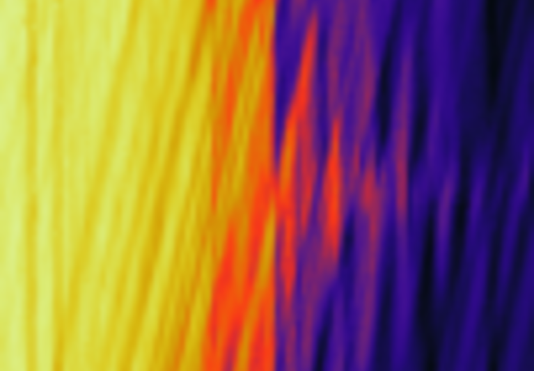
The picture shows basic overview of the whole field.
Quantum Conductance – One important scale in Quantum Transport
Conductance and energy scale are two most important measures in quantum transport. Quantum conductance GQ=e2/ π h is made of two fundamental constants, electron charge (most of quantum transport is related to the transport of electrons) and Plank constant (related to quantum mechanics). The energy scale is determined by adjustable experimental conditions (temperature kBT, bias applied to the nanostructure eV). Physical mechanisms do not necessarily depend on the size of the nanostructure; hover internal scales are dependent on it and they are bigger for smaller nanostructures.
Conductance quantum GQ is a universal measure of conductance. If G>>GQ many electrons travel through the nanostructure simultaneously and they can do it via transport channels. If G<<GQ transport takes place in rare discrete fashion, electrons tunnel one by one. The regions where G~GQ attract lot of interest.
Energy Scale – Another important scale in Quantum Transport
Nanostructures are characterized by several internal energy scales. Let’s assume that we have nanostructure which has the same size in all three dimensions and that it is connected to two leads that are much bigger than the nanostructure itself. If we now isolate it from the leads the electron energies will become discrete and exact positions of the energy levels will depend on the nanostructure itself. Typical energy distance between two levels is the mean level spacing δS. Additional energy scale relates to the fact that electrons are charged particles with an elementary charge e. Charging energy EC characterizes the interaction of electrons. It costs the charging energy to add an extra electron to the nanostructure.
Those two scales are relevant at low conductance. At high conductance electrons do not stay long enough in the nanostructure to sense those scales. If electrons go fast through the nanostructure this introduces new energy scale due to the quantum uncertainty principle, the Thouless energy ETh which is proportional to the conductance of the nanoparticle.
Additional line in the upper part of the graph is due to the electron-electron interaction and it limits the quantum mechanical coherence. On the right from the line we are dealing with classical incoherent transport. At the line the inelastic time is equal to the time the electron spends in the nanostructure. The energy scale can be estimated as δS~(G/GQ)2>>ETh. From the mesoscopic point of view Thouless has suggested that extended conductors can be well understood by subdividing a big conductor into smaller nanostructures. This is the reason why experiments dealing with mesoscopic effects are located in the vicinity of this line.
After introducing the borders different approaches can be chosen as a base for the studies.
Scattering Approach
One of the important concepts is scattering approach because at low energies any nanostructure can be seen as a huge scatterer for electron waves which come from the leads. For G>>GQ scattering approach extends to the mesoscopic boarder. At energies close to the Thouless energy dependence of the scattering matrix becomes relevant.
If we go up in the direction G>>GQ scattering theory becomes impractical due to the increase of the number of transport channels which increases the size of the scattering matrix. Alternative way to handle it is to self-average over quantum phases of the scattering matrix elements. As a result quantum laws governing this regime become similar to the laws of transport in classical electric circuits. Resulting quantum circuit theory “hides” quantum effects so that conductance could be treated by the classical Ohm’s law. This allows for the treatment of superconductivity, the statistics of electron transfers and spin transport in an “easier” way. Practically there is no limitation to quantum mechanics at high conductance as long one stays above mesoscopic border.
Charging Energy Scale
If we go into opposite direction G<<GQ the charging energy scale EC becomes more relevant. Strong interaction between the electrons must be taken into account. That is the reason why the focus is put on the energies of the order of EC and the mean level spacing δS is neglected. Single electron tunnelling regime is governed by the incoherent transfer of single electrons. Transfers are strongly correlated and can be precisely controlled; electrons can be manipulated one-by-one. Quantum correction to single-electron transport is called co-tunneling. The energy scale separates inelastic and elastic co-tunneling. In the elastic co-tunneling regime, the nanostructure can be regarded as ascatterer. The combination of the Coulomb blockade and superconductivity gives the opportunity to build quantum devices of almost macroscopic size.
Domain of low conductance and low energies of the order of the mean level spacing is related to the statistics of discrete electron levels. If we go up towards high conductance and stay left from the mesoscopic border we end up in the area with the universal conductance fluctuations and the interference correction to transport with weak localization. Strong localization is relevant for G<<GQ and high energies, where electron hopping becomes dominant mechanism of conduction.
Latest Approach in Transport Measurement
One of the newest developments is the use of nanostructures for quantum information storage and handling. In this case a flow of quantum information becomes relevant instead of a flow of quantum electrons. Qubits and quantum dots are most popular devices in quantum transport and their discrete nature of energy levels is essential. They occupy energy area of the level spacing δS on the map.
Some interaction effects do not fit into the simple framework of the Coulomb blockade. Lot of studies are focusing on the effects of an electromagnetic environment on electron tunnelling staying in the area of the Coulomb blockade. By going up along the conductance axis the role of the Coulomb blockade and interaction effects can be studied. The electrons in the leads provide environment which allows study of the Kondo effect in quantum dots. Energy dissipation can be discussed separately for qubits and electrons.
At high energies we are moving away from the field of quantum transport.
The numbered diamonds in the map refer ranges where some of the experiments were performed:
- Discovery of conductance quantization
- Interference nature of the weak localization
- Universal conductance fluctuations
- Single-electron transistor
- Discrete states in quantum dots
- Early qubit
- Kondo effect in quantum dots
- Energy relaxation in diffusive wires
Challenges of the Transport Measurement
Generally transport measurements are complex and time-critical requiring very low temperatures and very high signal performance on many signals simultaneously. In a typical measurement it takes lot of time to find working point on the sample even if the measurement itself is of no interest. The limiting factor is slow communication between instruments. This leads to the increase of the costs of Helium and electricity. Another disadvantage is that stability of the samples is often limited to a certain time scale.
Handling of the hardware and signals is also a complicated issue. A typical setup requires considerable space for DC sources, multi-meters, waveform generators, digitizer cards. Signal routing and summing are done in analogue domain compromising signal performance. Any change in the measurements configuration requires rewiring which could lead to sample damage.
Existing setups have often poor noise performance, insufficient resolution, large drift and some issues with low temperature. Higher measurement speed is possible but only by compromising on resolution, precision and noise performance. High performance instruments are usually single-channel and slow.
Signal analysis also requires additional instruments.
Solution for challenges
The solution for achieving higher measurement speeds and increasing safety for the samples without compromising on the performance is to do all signal processing and routing in the digital domain. Such solution allows open-signal architecture with full access to all signals at the same time. In such a solution sample would never need to be disconnected from the instrument so that no hardware handling would be necessary resulting in the increased safety for the sample. Such platform would be flexible and have upgradable software instruments instead of dedicated hardware.
In other words it is desirable to have more reliable and user friendly setups.
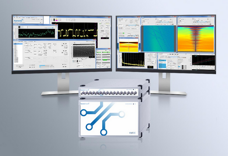
SPECS Nanonis Tramea was developed with this idea in mind. It is a modern and complete solution for time efficient measurements requiring handling of signals with high performance summing up all required hardware in only one box. It represents fully integrated digital system which avoids all complex wiring and where all operations are done via software making it comfortable to use and efficient in producing results. Base configuration hardware can be used as programmable DC sources, lock-in outputs, arbitrary waveform generators, multi-meters, lock in inputs, digitizers, oscilloscopes, spectrum analyzers, triggers… It comes with data acquisition and analysis tools. It can be extended with different software add-on modules like programming interface, lock-ins, high resolution oscilloscope, generic PI controller, function generator, scripting tool. Level of customizability is high and software based.
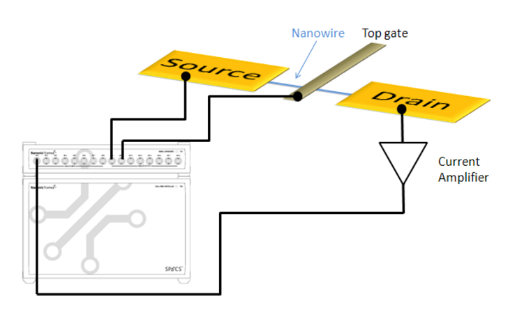
One application example would be reflectometry measurements. Nanonis Tramea allows fast quantum point contact readout, 100x100 pixel image can be acquired in 1 second. Such data acquisition speed allows complete characterization of the sample in a matter of seconds to minutes. Data generation and acquisition takes place in one system allowing easy optimization of measurement speed. Same data quality as with slow instruments is possible but with much shorter measurement time.
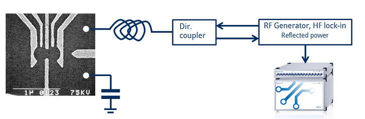
Hall-bar AC measurement can be done using one software lock-in module with multi-demodulator option instead of 5 hardware lock-ins results in a better performance simplified wiring, more flexibility and cost reducing. All input/output signals are handled with one system. Advanced filtering configurations improve signal performance significantly and reduce measurement time.

Some further examples where Nanonis Tramea was used for quantum transport measurements can be found in following application notes:
https://www.specs-group.com/nc/nanonis/products/detail/tramea/
https://www.specs-group.com/nc/specsgroup/knowledge/methods/detail/quantum-transport/