Logo specsDetail

KREIOS 150 S

Next Generation Electron Momentum Spectrometer for Small Spot ARPES and Momentum Microscopy

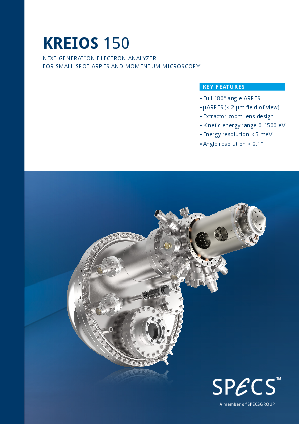
The KREIOS 150 S is a new generation of electron spectrometers for high performance ARPES and PEEM. The unique lens system combines an immersion lens for PEEM operation with a hemispherical energy analyzer scanning system for unrivaled ARPES measurements. Its lens system acquires the full half sphere of the electron emission for ultimate angular acceptance of 180°.

The KREIOS 150 S displays energy vs k-vector or energy vs spatial information directly on the detector. With the scanning lens it is possible to measure a full 3D dataset for ARPES or energy filtered PEEM. The lens system features apertures to refine the k-space into high contrast and dark field PEEM, as well as field apertures to select a spatial region for µ-ARPES down to 2 µm field of view. The kinetic energy up to 1500 eV allows XPS and XPEEM measurements. With the new CMOS detector, the KREIOS 150 S is the most performing ARPES analyzer available.

With a 2D CMOS detector it shows outstanding performance in count rate, linearity and a true pulse counting mechanism. It combines a state-of-the-art lens system with a proven hemisphere design for highest transmission and resolution.

The energy analyzer section is equipped with 8 customizable entrance and 3 exit slits. For highest energy and mapping resolution the entrance slit can be chosen down to 50 µm. The analyzer comes with a highly stable power supply, for best performance in a wide kinetic energy range.

This analyzer features the spectroscopy mode for data acquisition. For momentum microscopy a special MM and MM Twin version is available.

KEY FEATURES

  • Full 180° angle ARPES
  • µARPES (< 2 µm field of view)
  • Extractor zoom lens design
  • Kinetic energy range 0 - 1500 eV
  • Energy resolution < 5 meV
  • Angle resolution < 0.1°

Advanced ARPES

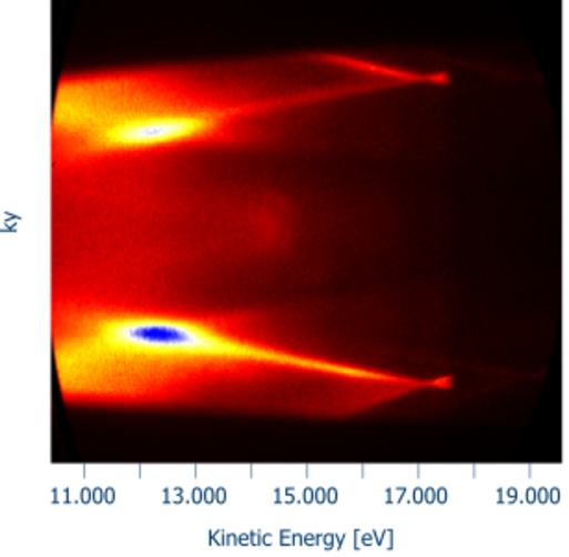
The KREIOS 150 allows to aquire photoemission data with a very large field of view. Thanks to the extraction field the full photoemission horizon is collected. The integarted momentum deflectors let you then scan teh full 3D valence band structure. 

PEEM

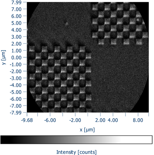
In PEEM mode, a real space image of the surface is aquired in energy dispersive mode. Line by line, a complete eneryg filtered PEEM image is aquired, whcih can be used to identify ares of interest on the sample. Here a secondary electron image of a chessboard test sample (Au/Si) is shown, showing best resolution <50 nm. 

XPEEM

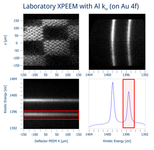
The KREIOS 150 was used for laboratory based XPEEM studies using a µFOCUS 500 monochromated x-ray source. The chessboard test sample (Au/Si) was measured on the Au 4f core level, revealinbg a clear chemcial contrast with respect to the substrate. 

Thanks to the high transmission of the PEEM lens combined with a hemispherical energy filter, teh KREIOS 150 is an ideal instrument for cpmbined chemical and electronic structure analysis. 

MADE FOR THESE METHODS

2

SPECIFICATIONS

KREIOS 150 S
Performance
Energy Resolution

< 5 meV

Angular Resolution

< 0.1° for 0.1 mm emission spot for He I

k-Resolution

0.008 Å-1 for 0.1 mm emission spot @ He I

Acceptance Angle

±90° full cone

Lateral Resolution

50 nm
35 nm Achievable

Smallest Acceptance Spot

2 µm

XPS Count Rates UHV

N/A

Detector Channels

1285 x 730 (with Channel Binning)

Operation
Kinetic Energy Range

0-1500 eV

Angular Resolved Modes

N/A

Pass Energies

1-200 eV Continuously Adjustable

Magnetic Shielding

Double µ-Metal Shielding

Energy Dispersion

Hemisphere

Lens Modes

PEEM Mode, Momentum Resolved Mode

Measurement Modes

Snapshot Mode, Sweeping Mode

Detector

2D CMOS Detector with Spin Option

Slits/Apertures

8 entrance and 3 exit slits and iris aperture

Energy Window

13% of Pass Energy

Electric Isolation

> 3.5 keV, 29 keV on lens system

Electronics

HSA + for KREIOS

Working Pressure

10-11 to 10-7 mbar

Mounting
Working Distance

4-10 mm

Mounting Flange

DN150CF (8" OD)

RELATED PRODUCTS

31

PUBLICATIONS

  1. (2023) Dirac Bands in the Topological Insulator Bi2Se3 Mapped by Time-Resolved Momentum Microscopy

    The energy dispersion of the unoccupied Dirac bands of the topological insulator Bi2Se3 has been studied up to large parallel momenta and intermediate state energies using a setup for laser-based time-resolved momentum microscopy with 6 eV probe-photons. A strongly momentum-dependent evolution of the topologically protected Dirac states into a conduction band resonance is observed, highlighting the anisotropy dictated by the symmetry of the surface. The results are in remarkable agreement with the theoretical surface spectrum obtained from a GW-corrected tight-binding model, suggesting the validity of the approach in the prediction of the quasiparticle excitation spectrum of large systems with non-trivial topology. After photoexcitation with 0.97 eV photons, assigned to a bulk valence band-conduction band transition, the out-of-equilibrium population of the surface state evolves on a multi-picosecond time scale, in agreement with a simple thermodynamical model with a fixed number of particles, suggesting a significant decoupling between bulk and surface states.


    Stefano Ponzoni, Felix Paßlack, Matija Stupar, David Maximilian Janas, Giovanni Zamborlini, Mirko Cinchetti
    Adv. Physics Res.2023, 2200016
    Read more
  2. (2019) Imaging properties of hemispherical electrostatic energy analyzers for high resolution momentum microscopy

    Hemispherical deflection analyzers are the most widely used energy filters for state-of-the-art electron spectroscopy. Due to the high spherical symmetry, they are also well suited as imaging energy filters for electron microscopy. Here, we review the imaging properties of hemispherical deflection analyzers with emphasis on the application for cathode lens microscopy. In particular, it turns out that aberrations, in general limiting the image resolution, cancel out at the entrance and exit of the analyzer. This finding allows more compact imaging energy filters for momentum microscopy or photoelectron emission microscopy. For instance, high resolution imaging is possible, using only a single hemisphere. Conversely, a double pass hemispherical analyzer can double the energy dispersion, which means it can double the energy resolution at certain transmission, or can multiply the transmission at certain energy resolution.


    C. Tusche, Y. J. Chen, C. M. Schneider and J. Kirschner
    Ultramicroscopy 206 (2019)
    Read more
  3. (2018) The graphene/n-Ge(110) interface: structure, doping, and electronic properties

    The implementation of graphene in semiconducting technology requires precise knowledge about the graphene–semiconductor interface. In our work the structure and electronic properties of the graphene/n-Ge(110) interface are investigated on the local (nm) and macro (from μm to mm) scales via a combination of different microscopic and spectroscopic surface science techniques accompanied by density functional theory calculations. The electronic structure of freestanding graphene remains almost completely intact in this system, with only a moderate n-doping indicating weak interaction between graphene and the Ge substrate. With regard to the optimisation of graphene growth it is found that the substrate temperature is a crucial factor, which determines the graphene layer alignment on the Ge(110) substrate during its growth from the atomic carbon source. Moreover, our results demonstrate that the preparation route for graphene on the doped semiconducting material (n-Ge) leads to the effective segregation of dopants at the interface between graphene and Ge(110). Furthermore, it is shown that these dopant atoms might form regular structures at the graphene/Ge interface and induce the doping of graphene. Our findings help to understand the interface properties of the graphene–semiconductor interfaces and the effect of dopants on the electronic structure of graphene in such systems.


    J. Tesch, F. Paschke, M. Fonin, M. Wietstruk, S. Böttcher, R. J. Koch, A. Bostwick, C. Jozwiak, E. Rotenberg, A. Makarova, B. Paulus, E. Voloshina, Y. Dedkov
    Nanoscale, 10, pp. 6088-6098
    Read more

DOWNLOADS

4
Close
Your web browser is deprecated
This could effect the presentation and some functions of our website.