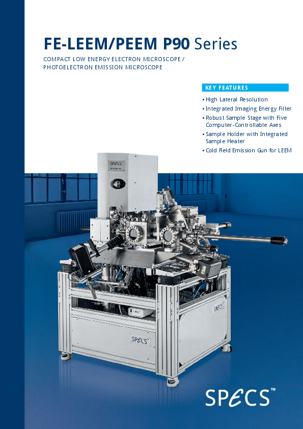
FE-LEEM/PEEM P90 NAP
High Pressure LEEM/PEEM System with up to 1 mbar Operational Pressure.
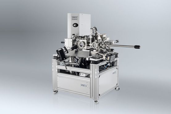
The SPECS FE-LEEM/PEEM P90 NAP system is a fully equipped UHV analysis system for modern surface microscopy. All systems are design and manufactured at the SPECS headquarter in Berlin. A special engineering group personally accompanies the system process from the order placing until the final acceptance. Our engineers are dedicated to highest quality and usability of the system during design, testing and setup on site. Once the system is in full operation a professional service team in our HQ and our worldwide branch offices takes care of a smooth and stable operation.
Low Energy Electron Microscopy and Photoelectron Emission Microscopy are the only electron microscopic methods that are really sensitive to the topmost layer of the surface. In combination with the spectroscopic information it is a unique tool for the characterization of dynamic processes at surfaces, like surface reactions. Often the pressure range of standard LEEM/PEEM is not sufficient. Furthermore solid/vapor and liquid/vapor interfaces are omnipresent in nature and the basis for important applications. Thus, investigations at near ambient pressure (NAP) conditions are a key to understanding processes at these interfaces. Analysis techniques like NAP-XPS can work at gas pressures orders of magnitude higher than typical ultra high vacuum conditions. Near Ambient Pressure LEEM and PEEM (NAP-LEEM/PEEM) is the new addition to the tool box, finally allowing for microscopic operando studies under NAP conditions down to the nanoscale.
SPARE PARTS
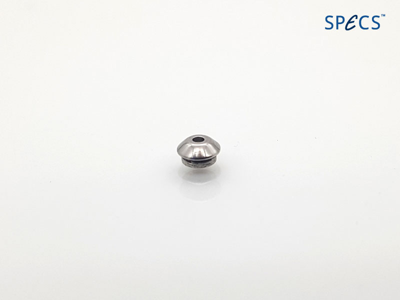
Special gasket for LEEM/PEEM sample chamber.
Isolation tube for LEEM/PEEM sample holder
1 mm nose insert for LEEM/PEEM transfer objective lens
Spare part set for LEEM/PEEM sample holder cap
4 mm Molybdenium sample holder cap for LEEM/PEEM
5 mm Molybdenium sample holder cap for LEEM/PEEM
LEEM/PEEM sample holder
Only suitable for systems in combination of LEEM/PEEM and Aarhus STM
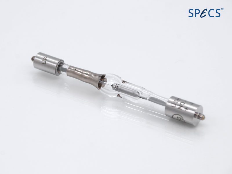
Replacement Halogen Lamp for LEEM/PEEM
Socket mount for sample holder LEEM