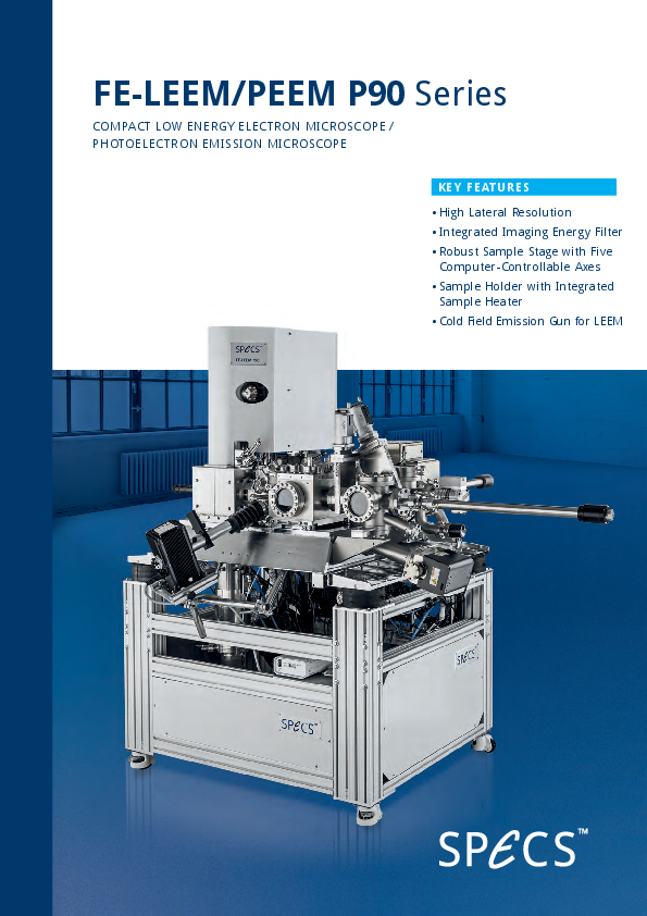
Logo specsDetail

FE-LEEM/PEEM P90 AC

The FE-LEEM/PEEM P90 AC is a combined LEEM and PEEM Instrument with Integrated Aberration Correction

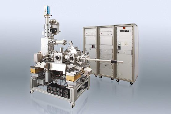
The SPECS FE-LEEM/PEEM P90 AC system is a fully equipped UHV analysis system for modern surface microscopy. All systems are designed and manufactured at the SPECS headquarter in Berlin. A special engineering group personally accompanies the system process from the order placing until the final acceptance. Our engineers are dedicated to highest quality and usability of the system during design, testing and setup on site. Once the system is in full operation a professional service team in our HQ and our worldwide branch offices takes care of a smooth and stable operation.

The SPECS LEEM instrument FE-LEEM P90 AC is a next generation Low Energy Electron Microscope with integrated aberration correction, showing astonishing 2 nm resolution for dynamic LEEM microscopy experiments. With this instrument, based on the design of Dr. Rudolf Tromp, nanometer scale processes on surfaces can be observed in real-time. 

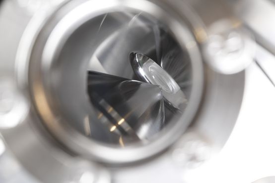
Guiding the design of the SPECS FE-LEEM P90 was the goal to achieve an extremely high resolution with a minimum number of electronoptical elements. 
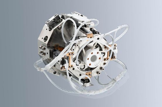
In order to achieve this incoming and outgoing electrons are separated by a 90° magnetic prism array. This geometry allows a simple, intuitive step by step adjustment of all lens parameters. The magnetic prism transfers both the LEEM image and the LEED pattern astigmatically, allowing routine switching between real image and diffraction. Both image and LEED pattern are transferred without the negative effects of chromatic dispersion, offering superior image and diffraction capabilities. 
A sophisticated energy filter enables imaging with an energy resolution down to 250 meV with a minimal impact on the high spatial resolution of the instrument. 
The FE-LEEM P90 is integrated into a UHV LEEM sample analysis chamber with facilities for sample preparation and in-situ high temperature sample processing.

KEY FEATURES

  • 2 nm resolution in AC-LEEM mode
  • 90° magnetic deflector
  • Cold Field emitter
  • Energy filter (optional)
  • Rapid LEED/LEEM switching
  • Fast sample exchange
  • Energy filtered PEEM with focussing UV source UVS 300

MADE FOR THESE METHODS

1

SPECIFICATIONS

FE-LEEM/PEEM P90 AC
Performance
Lateral Resolution

3 nm Guaranteed, 1.6 achievable (LEEM) 
8 nm (PEEM)

Energy Resolution

< 250 meV (Spectroscopy)
< 1.7 eV (Imaging)

Field of View

800 nm - 100 µm

Base Pressure

< 2x10⁻¹⁰ mbar

Sample Temperature

RT - 1500 K
150 K optionally available

Spot Size

< 40 µm - < 200 nm
(LEEM with micro diffraction aperture)

Lateral Stability

< 5 nm

Lateral Reprodicibility

< 500 nm

Operation
Magnification

400x - 5000x

Kinetic Energy Range

0-1000 eV

Extraction Voltage

2 keV - 15 keV

Electron Gun

Cold Field Emission Gun
with < 300 meV Energy Width

Mounting
Energy Filter

90° Magnetic Prism

Slits/Apertures

Integrated Contrast and Field Apertures

Sample Holder

SPECS SH2/12
Stub Sample Holder

Aberration Correction

Additional 90° Magnetic Prism
with Correction Optics

APPLICATION NOTES

PUBLICATIONS

  1. (2021) Stacking Relations and Substrate Interaction of Graphene on Copper Foil

    The crystallinity of graphene flakes and their orientation with respect to the Cu(111) substrate are investigated by means of low-energy electron microscopy (LEEM). The interplay between graphene and the metal substrate during chemical vapor deposition (CVD) introduces a restructuring of the metal surface into surface facets, which undergo a step bunching process during the growth of additional layers. Moreover, the surface facets introduce strain between the successively nucleated layers that follow the topography in a carpet-like fashion. The strain leads to dislocations in between domains of relaxed Bernal stacking. After the transfer onto an epitaxial buffer layer, the imprinted rippled structure of even monolayer graphene as well as the stacking dislocations are preserved. A similar behavior might also be expected for other CVD grown 2D materials such as hexagonal boron nitride or transition metal dichalcogenides, where stacking relations after transfer on a target substrate or heterostructure could become important in future experiments.


    P. Schädlich, F. Speck, C. Bouhafs, N. Mishra, S.Forti, C. Coletti, and T. Seyller
    Adv. Funct. Mater, Volume 8, Issue 7, April 9, 2021, 2002025
    Read more
  2. (2020) Silicon Carbide Stacking-Order-Induced Doping Variation in Epitaxial Graphene

    Generally, it is supposed that the Fermi level in epitaxial graphene is controlled by two effects: p-type polarization doping induced by the bulk of the hexagonal silicon carbide (SiC)(0001) substrate and overcompensation by donor-like states related to the buffer layer. The presented work is evidence that this effect is also related to the specific underlying SiC terrace. Here a periodic sequence of non-identical SiC terraces is fabricated, which are unambiguously attributed to specific SiC surface terminations. A clear correlation between the SiC termination and the electronic graphene properties is experimentally observed and confirmed by various complementary surface-sensitive methods. This correlation is attributed to a proximity effect of the SiC termination-dependent polarization doping on the overlying graphene layer. These findings open a new approach for a nano-scale doping-engineering by the self-patterning of epitaxial graphene and other 2D layers on dielectric polar substrates.


    D. M. Pakdehi, P. Schädlich, T. T. N. Nguyen, A. A. Zakharov, S. Wundrack, E. Najafidehaghani, F. Speck, K. Pierz, T. Seyller, C. Tegenkamp, and H. W. Schumacher
    Adv. Funct. Mater, Volume 30, Issue 45, November 4, 2020, 2004695
    Read more
  3. (2015) Low-Energy Electron Potentiometry: Contactless Imaging of Charge Transport on the Nanoscale

    Charge transport measurements form an essential tool in condensed matter physics. The usual approach is to contact a sample by two or four probes, measure the resistance and derive the resistivity, assuming homogeneity within the sample. A more thorough understanding, however, requires knowledge of local resistivity variations. Spatially resolved information is particularly important when studying novel materials like topological insulators, where the current is localized at the edges, or quasi-two-dimensional (2D) systems, where small-scale variations can determine global properties. Here, we demonstrate a new method to determine spatially-resolved voltage maps of current-carrying samples. This technique is based on low-energy electron microscopy (LEEM) and is therefore quick and non-invasive. It makes use of resonance-induced contrast, which strongly depends on the local potential. We demonstrate our method using single to triple layer graphene. However, it is straightforwardly extendable to other quasi-2D systems, most prominently to the upcoming class of layered van der Waals materials.


    J. Kautz, J. Jobst, C. Sorger, R. M. Tromp, H. B. Weber und S. J. van der Molen
    Scientific Reports volume 5, Article number: 13604 (2015)
    Read more

SPARE PARTS

10
Product image
Product description
Article No.
 
Gasket Helicoflex for LEEM Sample chamber

Special gasket for LEEM/PEEM sample chamber.

2060004567
Isolation tube sample holder LEEM

Isolation tube for LEEM/PEEM sample holder

2055001665
Nose insert 1 mm for objective lens

1 mm nose insert for LEEM/PEEM transfer objective lens

2055001905
Sample holder cap spares set

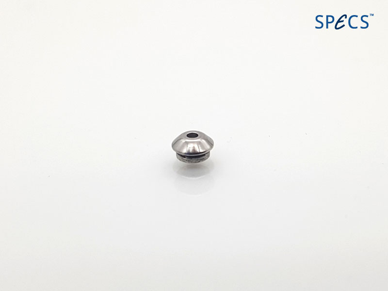
Spare part set for LEEM/PEEM sample holder cap

2055006884
Sample holder cap, Mo, 4 mm

4 mm Molybdenium sample holder cap for LEEM/PEEM

2055019253
Sample holder cap, Mo, 5 mm

5 mm Molybdenium sample holder cap for LEEM/PEEM

2055001664
Sample holder LEEM

LEEM/PEEM sample holder

2055017420
Sample holder LEEM-Aarhus

Only suitable for systems in combination of LEEM/PEEM and Aarhus STM

2100004650
Short-arc Hg halogen lamp, 100 W

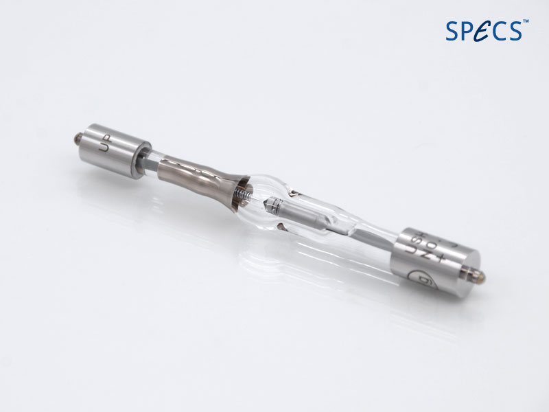
Replacement Halogen Lamp for LEEM/PEEM

2060004220
Socket mount for sample holder LEEM

Socket mount for sample holder LEEM

2055001652

DOWNLOADS

9
Close
Your web browser is deprecated
This could effect the presentation and some functions of our website.