Logo specsDetail

ErLEED 150

LEED Optics for Structural Analysis and AES with Miniature Electron Gun for Increased Field of View, High Transmission Grid Assembly and Digital or Analog Control Unit

Low Energy Electron Diffraction (LEED) is one of the most powerful methods to determine surface structures. Analysis of LEED patterns and intensities provides the size and shape of the surface unit cell, the degree of order and detailed atomic structure with a precision of the order of picometers. To exploit the full power of the technique, equally capable instrumentation is required.  

The SPECS reverse view ErLEED optics together with highly sophisticated acquisition and analysis solutions provide the experimenter with many unique advantages present in no other commercial unit. In order to guarantee the highest possible quality and performance of each optics, great importance is attached to the selection of the materials and components as well as to the quality of the mechanical and electrical manufacturing.

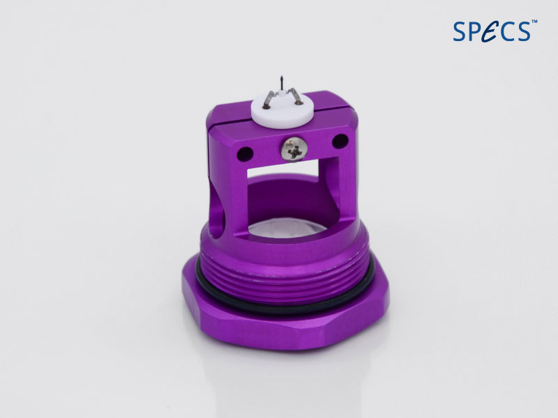
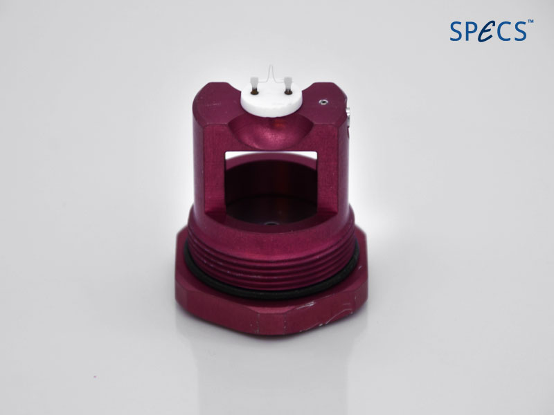
The miniature electron gun allows a full view of the diffraction pattern. It is completely light shielded in order to avoid stray light and thus to be able to measure quantitative LEED I(E) curves or spot profiles. Two types of filaments are available: Thoria coated Iridium hairpin and LaB6 single crystal. The Thoria coated Iridium filaments allow the operation of the gun at pressures of up to 10-4 mbar. All filaments are easily replaceable in the users laboratory. The high transmission grid assemblies are made of Gold coated Molybdenum ensuring long term rigidity of the hemispheres as well as an uniform work function and non-magnetic characteristics. The optics is available in a 2, 3 and 4 grid version.  ErLEED 150 is mounted on a DN150CF flange (8“ CF, 203 mm OD). A z-retraction mechanism allows the optics to be extended or withdrawn from a restricted working area. Z-travel of 50 mm or 100 mm is available. The optics can be protected by an integral multi-segment shutter mounted in front of all grids. All ErLEED optics are fully tested under UHV conditions before delivery. A detailed test certificate is supplied with each optics.

KEY FEATURES

  • High performance optics for LEED and AES
  • Mounted on DN150CF (8“OD) flange
  • Light shielded miniature electron gun
  • 50 or 100 mm z-retraction (optional)
  • Integral multi-segment shutter (optional)
  • Digitally or analog controlled power supplies with independent HV modules

MADE FOR THESE METHODS

2

SPECIFICATIONS

ErLEED 150
Mounting
Mounting Flange

DN150CF (8 ")

Insertion Depth

165 mm, 203 mm, 254 mm, 354 mm

Z-Retraction

optional 50/100 mm

Shutter

optional

Power Supply

  • ErLEED 1000A analog for LEED
  • ErLEED 3000D digital for LEED/AES
Operation
Screen Voltage

  • 0 - 7.5 kV for ErLEED 1000A
  • 0-10 kV for ErLEED 3000D

Primary Energy

  • 0 - 1000 eV for LEED
  • 0 -3000 eV for AES

Operating Pressure

< 10-9 - 10-4 mbar

Optional Accessories

  • Integrated shutter
  • Non standard lengths
  • Thoria coated Iridium hairpin filament
  • LaB6 single crystal filament

PUBLICATIONS

  1. (2021) Epitaxial thin-film Pd1−xFex alloy: a tunable ferromagnet for superconducting spintronics

    Thin epitaxial films of the palladium-rich Pd1−xFex alloy were synthesized and extensively studied as a tunable ferromagnetic material for superconducting spintronics. The (001)-oriented MgO single-crystal substrate and the composition range of x = 0.01–0.07 were chosen to support the epitaxial growth and provide the films with magnetic properties spanning from very soft ferromagnet for memory applications to intermediately soft and moderately hard for the programmable logic and circuit biasing, respectively. Dependences of the saturation magnetization, Curie temperature and three magnetic anisotropy constants on the iron content x were obtained for the first time from the analyses of the magnetometry and ferromagnetic resonance data. The experimental results were discussed based on existing theories of dilute ferromagnetic alloys. Simulation of the hysteresis loops within the Stoner-Wohlfarth model indicates the predominant coherent magnetic moment rotation at cryogenic temperatures. The obtained results were compiled in a database of magnetic properties of a palladium-iron alloy in a single-crystal thin-film form considered as a material for superconducting spintronics.


    A. Esmaeili, I. V. Yanilkin, A. I. Gumarov, I. R. Vakhitov, B. F. Gabbasov, R. V. Yusupov,
    D. A. Tatarsky, and L. R. Tagirov
    Science China Materials volume 64, pages 1246–1255 (2021)
    Read more
  2. (2021) Synthesis, Characterization, and Magnetoresistive Properties of the Epitaxial Pd0.96Fe0.04 /VN/Pd 0.92 Fe 0.08 Superconducting Spin-Valve Heterostructure

    A thin-film superconductor(S)/ferromagnet(F) F1/S/F2-type Pd0.96Fe0.04 (20 nm)/VN(30 nm)/Pd0.92Fe0.08 (12 nm) heteroepitaxial structure was synthesized on (001)-oriented single-crystal MgO substrate utilizing a combination of the reactive magnetron sputtering and the molecular-beam epitaxy techniques in ultrahigh vacuum conditions. The reference VN film, Pd0.96Fe0.04 /VN, and VN/Pd0.92 Fe0.08 bilayers were grown in one run with the target sample. In-situ low-energy electron diffraction and ex-situ X-ray diffraction investigations approved that all the Pd1−xFex and VN layers in the series grew epitaxial in a cube-on-cube mode. Electric resistance measurements demonstrated sharp transitions to the superconducting state with the critical temperature reducing gradually from 7.7 to 5.4 K in the sequence of the VN film, Pd0.96 Fe0.04 /VN, VN/Pd0.92Fe0.08 , and Pd0.96Fe0.04 /VN/Pd0.92Fe0.08 heterostructures due to the superconductor/ferromagnet proximity effect. Transition width increased in the same sequence from 21 to 40 mK. Magnetoresistance studies of the trilayer Pd0.96Fe0.04 /VN/Pd0.92 Fe0.08 sample revealed a superconducting spin-valve effect upon switching between the parallel and antiparallel magnetic configurations, and anomalies associated with the magnetic moment reversals of the ferromagnetic Pd0.92Fe0.08 and Pd0.96Fe0.04 alloy layers. The moderate critical temperature suppression and manifestations of superconducting spin-valve properties make this kind of material promising for superconducting spintronics applications.


    I. Yanilkin, W. Mohammed, A. Gumarov, A. Kiiamov, R. Yusupov, and L. Tagirov
    Nanomaterials 2021, 11, 64
    Read more
  3. (2019) Epitaxial growth of Pd1−x Fex films on MgO single-crystal substrate

    In the paper we report on growth conditions, morphology, crystallographic structure and magnetic anisotropy of 20 nm thick, palladium-rich Pd1−xFex (0.01 < x < 0.1) alloy films grown on (001)-oriented MgO single-crystal substrate. Molecular beam deposition at ultra-high vacuum conditions has been utilized along with the three-step procedure to achieve the epitaxy conditions for the synthesized films. The scanning electron microscopy and atomic force microscopy have shown flat and smooth morphology of the films studied in a wide range of lateral scales. In situ low energy electron diffraction and ex situ X-ray diffraction measurements confirmed that our Pd1−xFex alloy films are epitaxial. Ferromagnetic resonance investigations have shown the in-plane four-fold magnetocrystalline anisotropy characteristic for single-crystalline films with the cubic structure. The whole set of our measurements testifies the epitaxial cube-on-cube growth and excellent magnetic homogeneity of Pd1−xFex films on MgO substrate obtained within the three-step deposition process.


    A. Esmaeilia, I.V. Yanilkina, A.I. Gumarova, I.R. Vakhitova, B.F. Gabbasova, A.G. Kiiamova,
    A.M. Rogova, Yu.N. Osina, A.E. Denisova, R.V. Yusupova, and L.R. Tagirova
    Thin Solid Films 669 (2019) 338–344
    Read more
  4. (2000) Three-dimensional band mapping by angle-dependent very-low-energy electron diffraction and photoemission: Methodology and application to Cu

    A method of band mapping providing full control of the three-dimensional k is described in detail. Angle-dependent very-low-energy electron diffraction is applied to determine the photoemission final states along a Brillouin zone symmetry line parallel to the surface; photoemission out of these states is then utilized to map the valence bands in the constant-final-state mode. The method naturally incorporates the non-free-electron and excited-state self-energy effects in the unoccupied band, resulting in an accuracy superior over conventional techniques. Moreover, its intrinsic accuracy is less limited by lifetime broadening. As a practical advantage, the method provides access to a variety of lines in the Brillouin zone using only one crystal surface. We extensively tested the method on Cu. Several new aspects of the electronic structure of this metal are determined, including non-free-electron behavior of unoccupied bands and missing pieces of the valence band.


    V.N. Strocov, R. Claessen, G. Nicolay, S. Hüfner, A. Kimura, A. Harasawa, S. Shin, A. Kakizaki, P. O. Nilsson, H. I. Starnberg, P. Blaha
    Phys. Rev. B. 63, 205108 ff.
    Read more
  5. (1998) Absolute Band Mapping by Combined Angle-Dependent Very-Low-Energy Electron Diffraction and Photoemission: Application to Cu

    We present an experimental method to determine the electronic E(k) band structure in crystalline solids absolutely, i.e., with complete control of the three-dimensional wave vector k. Angle-dependent very-low-energy electron diffraction is first applied to determine the unoccupied states whose k is located on a high-symmetry line parallel to the surface. Photoemission via these states, employing the constant-final-state mode, is then utilized to map the valence bands along this line. We demonstrate the method by application to Cu, and find significant deviation from free-electron-like behavior in the unoccupied states, and from density-functional theory in the occupied states.


    V. N. Strocov, R. Claessen, G. Nicolay, S. Hüfner, A. Kimura, A. Harasawa, S. Shin, A. Kakizaki, P. O. Nilsson, H. I. Starnberg, P. Blaha
    Phys. Rev. Lett. 81 (22), pp. 4943ff.
    Read more
  6. (1996) Electrostatic ray-tracing calculations in VLEED

    The present ray-tracing scheme employs the electrostatic potential calculation by finite-difference solution of the Laplace equation in three dimensions. The run time reduction, achieved by using successively refined grids and optimizing the iteration cycle, allows one to perform calculations on a personal computer. The code is applied to a standard four-grid LEED optics, operated in the retarding field mode, to calculate electron trajectories in the case of off-symmetry incidence. In particular, dependences of incidence on the sample rotation and primary energy are calculated. A simple empirical formula is derived, which allows accurate experimental determination of without extensive calculations. Ray-tracing calculations are further applied to analyse the influence of residual asymmetries of the electron optics.


    V.N. Strocov
    Meas. Sci. Technol. 7, pp. 1636-1642
    Read more

SPARE PARTS

6
Product image
Product description
Article No.
 
Set of ceramics for ErLEED 150/100 4-grids

Set of Ceramics for SCREEN/grid package. Comprising 4 x ceramic stubs plus all distance ceramics

2060006052
ErLEED screen for optics DN150CF (8")

ErLEED screen for optics DN150CF (8") coated with conductive layer and phosphor

2000203120
LaB6 cathode for ErLEED-optics

LaB6 cathode for ErLEED-optics, for long lifetime and small heating temperature, only for use in UHV. (do not use this filament in non baked vacuum and when using oxygen within the vacuum chamber)

2000204120
Nut for retraction of ErLEED

Nut for spindle of retraction of ErLEED 150 or 100

2060014098
Rotary feedthrough ErLEED 150

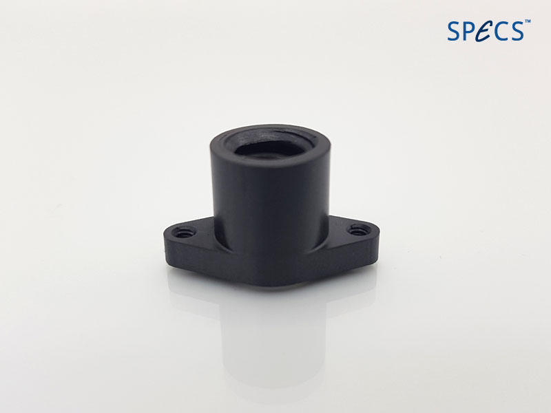
Rotary feedthrough ErLEED 150 for Z-retraction ( with coupling)

2100012246
Thoria coated Iridium-Filament

Thoria coated Iridium-Filament for ErLEED , standard filament also for work in non baked vacuum.

2000204110

DOWNLOADS

2
Close
Your web browser is deprecated
This could effect the presentation and some functions of our website.