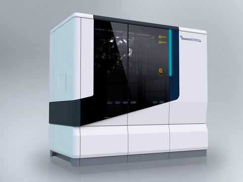
EnviroMETROS FAB
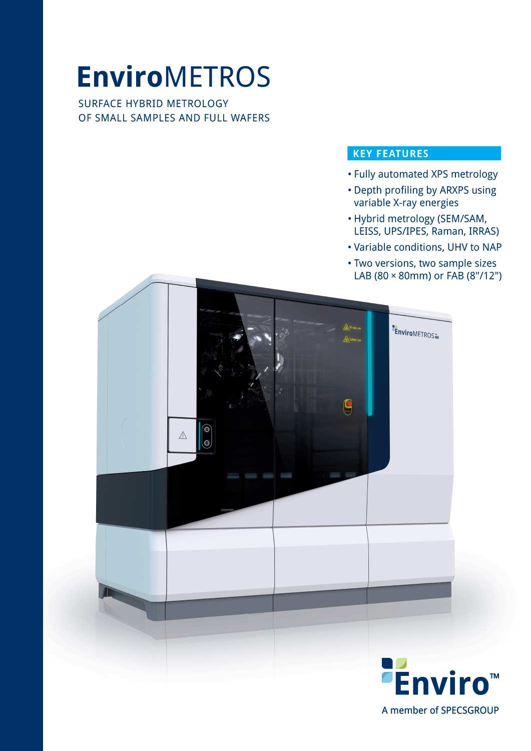
The novel EnviroMETROS series provides the perfect routine analysis tools for any sample with a special focus on multilayer thin films and their surfaces by combining small to large sample capabilities or wafer handling with a variable information depth photoelectron spectrometer.
EnviroMETROS is a unique metrology platform for the chemical analysis of ultrathin films and 2D materials that allows a detailed characterization of stoichiometries‚ composition and depth distribution of elements. In combination with optical and other analytical techniques it enables depth dependent composition analysis of unsurpassed precision‚ reliability and repeatability.
KEY FEATURES
- Metrology with ultimate stability, reliability and repeatability;
- Precise chemical and
dimensional quantification - Short acquisition times
(high sensitivites and throughput) - Non-destructive depth profiling using different photon energies in combination with angle resolved XPS (ARXPS)
- Flexible analysis area (100 µm to 1 mm)
- Integration of supplementary optical metrology (IRRAS and Raman)
- Electronic structure analysis
by combined UPS and IPES - Identification of energy loss
mechanisms by REELS - Option to operate the system in
UHV or NAP environment - Fully Software Controlled
SPECIFICATIONS
EnviroMETROS FAB
Configuration
| System |
|
| EnviroMETROS FAB 8 and FAB 12 System |
|
| Pumping System |
|
| Electron spectrometer |
|
| Electron spectrometer |
|
| X-Ray Source |
|
| Charge neutralization |
|
| SEM/SAM |
|
| Sputter depth profiling |
|
| LEISS |
|
| (NAP-)UPS |
|
| IPES |
|
| REELS |
|
| Raman/IRRAS |
|
| Gas dosing system |
|
| Automation |
|
| Software |
|
| Wafer size |
|
| Samples |
|
| Electrical contacts |
|
| Sample stage |
|
Your web browser is deprecated
This could effect the presentation and some functions of our website.